Nvidia Quietly Shrank Vera Rubin's Spec Sheet. Here's What It Means
Nvidia trimmed Vera Rubin's published memory and NVLink bandwidth by 11% to 26% in September, without an announcement, just as the racks hit general availability at Oracle. I checked the archived pages myself. Here's what changed, what Nvidia says, why memory bandwidth is the spec that matters most for serving AI, and what it means for buyers and for AMD.
Tom Pechulis, , 12 min read
The last three posts were about money: what GPU debt costs, Nvidia co-signing Nscale's debt, and Anthropic's $895B compute bill. Today is about what all that money actually buys. Nvidia has lowered the published memory and interconnect bandwidth of Vera Rubin, its newest AI system, by 11% to 26%. There was no announcement. Dataconomy wrote it up yesterday (Dataconomy, Nov 2), following Wccftech, TrendForce, and ServeTheHome over the past week. I didn't want to take anyone's word for it, so I pulled Nvidia's live pages and the Wayback Machine snapshots myself.
TL;DR
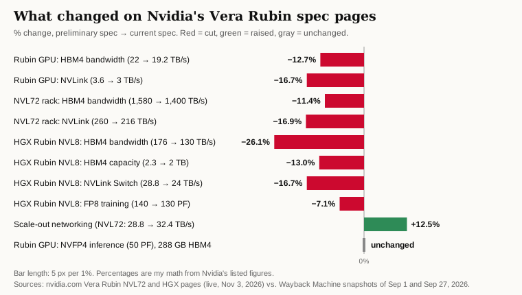
- Confirmed on Nvidia's own pages: each Rubin GPU's memory bandwidth went from 22 to 19.2 TB/s and its NVLink went from 3.6 to 3 TB/s. The 72-GPU rack went from 1,580 to 1,400 TB/s of memory bandwidth and from 260 to 216 TB/s of NVLink. The 8-GPU HGX server took the biggest cut: 176 → 130 TB/s (−26%), and 2.3 → 2 TB of memory (current page vs. Sep 1 snapshot; HGX page vs. Sep 27 snapshot).
- Unchanged: the headline compute (50 PFLOPS of NVFP4 per GPU) and 288 GB of memory per GPU. Raised: scale-out networking, +12.5%.
- When: the rack page changed between Sep 1 and Sep 11. The HGX page changed later, between Sep 27 and Oct 1 (my check of the archive; dates in PT).
- Nvidia's line: the old numbers were "preliminary architectural targets," and the new ones "reflect what the system sustains at qualified, volume production" (Nvidia via Wccftech). Nvidia hasn't said why the targets were missed.
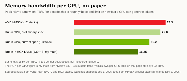
- Why it matters: memory bandwidth sets the speed limit for the part of AI serving where the model writes its answer. On paper, AMD's MI455X now has about 21% more bandwidth per GPU than Rubin (my math: 23.3 ÷ 19.2).
Quick jargon decoder
| Term | Plain English |
|---|---|
| HBM (HBM4) | High-bandwidth memory: stacks of memory chips sitting right next to the GPU. HBM4 is the newest generation. I wrote about why it's the real capacity constraint. |
| TB/s | Terabytes per second: how much data can move each second. 19.2 TB/s is roughly 19,200 gigabytes every second. |
| Memory bandwidth | How fast the GPU can read from its memory. Capacity (GB) is the size of the warehouse. Bandwidth is the width of the loading dock. |
| NVLink | Nvidia's high-speed link that lets GPUs in one system talk to each other as if they were one giant GPU. |
| Scale-up vs. scale-out | Scale-up is GPUs inside one NVLink system (up to 72 in a rack). Scale-out is the regular network that connects racks to each other. |
| NVFP4 | Nvidia's 4-bit number format. Using fewer bits per number lets the chip do more math per second. That's where the "50 PFLOPS" headline comes from. |
| Prefill vs. decode | Prefill is the model reading your prompt, all at once. Decode is the model writing its answer, one token (a word-chunk) at a time. |
| NVL72 / HGX NVL8 | NVL72 is the 72-GPU rack that works as one system. HGX NVL8 is the classic 8-GPU server. More on that shift here. |
What changed, exactly
Here's the rack page's spec table, comparing the Sep 1 archived copy with the Sep 11 copy and with the live page this morning:
| Spec | Before (Sep 1) | Now | Change (my math) |
|---|---|---|---|
| Rubin GPU memory bandwidth | 22 TB/s | 19.2 TB/s | −12.7% |
| Rubin GPU NVLink | 3.6 TB/s | 3 TB/s | −16.7% |
| Superchip (2 GPUs) memory bandwidth | 44 TB/s | 38.5 TB/s | −12.5% |
| NVL72 rack memory bandwidth | 1,580 TB/s | 1,400 TB/s | −11.4% |
| NVL72 rack NVLink | 260 TB/s | 216 TB/s | −16.9% |
| NVL72 scale-out networking | 28.8 TB/s | 32.4 TB/s | +12.5% |
| Memory per GPU / per rack | 288 GB / 20.7 TB | 288 GB / 20.7 TB | none |
| NVFP4 inference per GPU | 50 PFLOPS | 50 PFLOPS | none |
A few quieter edits in the same table caught my eye:
- The footnote that said "Preliminary information. All values are up to and subject to change" is gone. It has been replaced by "Specifications based on an at-scale AI factory using NVIDIA DSX with MaxLPS."
- The INT8 row and the emulated FP32/FP64 matrix-math rows were dropped from the rack table.
- The rack's CPU memory went from "54 TB" to "Up to 54 TB." TrendForce, citing IT Home, flagged the same "up to" change for the Vera CPU (TrendForce, Oct 27).
The 8-GPU HGX server got hit harder. Comparing the Sep 27 snapshot with the Oct 1 snapshot and the live HGX page:
- Memory: 2.3 TB → 2 TB. Memory bandwidth: 176 → 130 TB/s (−26.1%, my math).
- NVLink Switch bandwidth: 28.8 → 24 TB/s.
- Dense training compute: 280 → 270 PFLOPS NVFP4 and 140 → 130 PFLOPS FP8.
- Networking: 1.6 → 1.8 TB/s.
- The marketing copy changed from "3x more memory bandwidth at 176 TB/s" to "2.1x more memory bandwidth at 130 TB/s."
One oddity: the HGX page's per-GPU table still says 22 TB/s and 3.6 TB/s today, which doesn't match its own system totals. Divide 130 TB/s across 8 GPUs and you get ~16.25 TB/s each (my math). ServeTheHome's read is that 2 TB works out to roughly 250 GB per GPU, which "requires only 7 of the GPU's 8 HBM4 memory stacks," for about 16.8 TB/s per GPU (ServeTheHome, Oct 31). That's STH's inference, not something Nvidia has said.
Correction to some coverage: this isn't brand-new. The rack edits date to early September. Then IT Home spotted them (per STH), TrendForce wrote it up on Oct 27, and Dataconomy did on Nov 2. "Quietly" is accurate. "This week" isn't.
The timing: Rubin is going live
The spec change is surfacing just as Rubin reaches customers. On Oct 27, Nvidia and Oracle announced that Vera Rubin NVL72 is generally available on Oracle Cloud (OCI), with plans to expand to "multi-gigawatt scale." Oracle also plans to offer the HGX Rubin NVL8 in an x86 server with two 64-core Xeon 6 CPUs and 4 TB of DDR5 (Nvidia newsroom, Oct 27; Oracle). No gigawatt number was given. (I've seen the announcement dated Nov 2 elsewhere. Both companies' releases say Oct 27.)
Oracle's own blog still describes Vera Rubin NVL72 as having "ultra-fast HBM4 memory" that "effectively eliminates data-movement bottlenecks" (Oracle blog, Oct 27). So the system that's now on sale is the 19.2 TB/s version. And the HGX box Oracle is planning is the one that lost the most bandwidth on paper.
What Nvidia says
Nvidia's statement to Wccftech (Oct 29):
"The specifications published during Vera Rubin's development were preliminary architectural targets. Final specifications on nvidia.com and the Vera Rubin datasheet reflect what the system sustains at qualified, volume production."
Nvidia also said "individual component specifications do not determine application performance." It said third-party benchmarks "available for months" were measured on production specs and show "30x more performance per watt and 30x more tokens per dollar versus the previous-generation GB300 NVL72," and it pointed readers to SemiAnalysis's AgentX and Artificial Analysis's AgentPerf.
That's a fair point, and it's the most important one in the whole story. If the published benchmarks were run on shipping hardware, the measured results already include the lower bandwidth. What changes is the spec sheet, not the silicon customers receive.
Why did the numbers drop? (Mostly unconfirmed)
Nvidia hasn't explained it. Here's what's actually on the record:
- The math is simple. A Rubin GPU has 8 HBM4 stacks, each with a 2,048-bit interface. Per ServeTheHome, 22 TB/s means running each pin at about 10.75 Gb/s, and 19.2 TB/s means about 9.375 Gb/s (STH). My math checks: 8 × 2,048 × 9.375 ÷ 8 bits per byte = 19,200 GB/s.
- Both numbers are well above the standard. The official JEDEC HBM4 spec targets 8 Gb/s per pin (STH; Dataconomy). Nvidia was pushing memory harder than the standard, and it's still doing so after the cut.
- The memory makers say their parts are fast enough. Samsung and SK hynix have disclosed 11.7 Gb/s per pin, and Micron "exceeding 11 Gbps," which in theory would meet the original target, according to Economy Tribune via TrendForce. IT Home notes that a lower bar "could allow more HBM4 products to qualify," which could boost output (same source).
- Speculation, clearly labeled: STH says the "immediate assumption" is that Nvidia and its suppliers couldn't hit the target, whether because of the memory controller, stack speeds, or yields (how many stacks run at the target speed), or some combination. That's an educated guess, not a confirmed cause. My own guess, also unconfirmed: a lower bar means more of the HBM supply qualifies, and in a market where HBM is the bottleneck, shipping more GPUs at 19.2 probably beats shipping fewer at 22.
Some outlets have offered more specific explanations, like exact signaling-frequency changes, without citing a source. I've left those out.
Why memory bandwidth is the spec that matters
Here's the plain-English version. When a chatbot writes an answer, it produces one token at a time, and for every token the GPU has to read the model's weights (and the conversation so far) out of memory. The math per token is light. The data movement is heavy. So the speed limit is usually how fast you can read memory, not how fast you can do math.
Nvidia says this itself. Its July Rubin architecture post calls decode "fundamentally memory subsystem bound," then adds: "It is not about peak bandwidth specs but rather how efficiently each kernel can utilize the entire memory subsystem" (Nvidia Technical Blog, Jul 21). That post still says "up to 22 TB/s" today.
My math: a toy example (hypothetical inputs, not a real model). Imagine a model that has to read 50 GB from memory for every token, for example 100B active parameters at 4 bits each. Serving one user at a time, the best-case speed is bandwidth ÷ bytes per token:
- At 22 TB/s: 22,000 ÷ 50 = 440 tokens/sec
- At 19.2 TB/s: 19,200 ÷ 50 = 384 tokens/sec
That's the same −12.7% as the bandwidth. Real systems land below these ceilings, and batching many users shares the weight reads. But for decode-heavy work, the ceiling moves roughly in proportion to bandwidth. Prefill and training lean harder on compute, which didn't change, so they should be far less affected.
The NVLink cut (−17%) matters most for giant mixture-of-experts models split across all 72 GPUs in a rack, because those GPUs constantly pass data to each other. More scale-out bandwidth (+12.5%) helps traffic between racks, but it's a different pipe.
What it means for buyers and neoclouds
If you're paying for Rubin by the GPU-hour (see what a GPU-hour really costs), here's the sensitivity, in my math:
- Same price, less bandwidth. If a Rubin GPU-hour costs the same as it did when everyone was modeling 22 TB/s, you're paying ~14.6% more per unit of memory bandwidth (22 ÷ 19.2 = 1.146). On the HGX NVL8 the figure is ~35% (176 ÷ 130 = 1.354).
- Who should re-run their numbers: anyone whose business case or capacity plan came from the spec sheet rather than measured benchmarks. That includes some neocloud pitch decks and lender models. A decode-heavy inference business modeled at 22 TB/s could see a token-per-GPU ceiling up to ~13% lower than planned (my math, from the toy example above).
- Who probably shouldn't panic: buyers who priced off measured, third-party benchmarks. If Nvidia is right that those were run on production hardware, they've already priced it in.
- The question I'd ask a vendor: "Which spec revision is your price-per-token quote based on, and was it measured on shipping hardware?"
For Nvidia's marketing claims, the rack page still promises "up to 10x more tokens per megawatt" and "one-tenth the cost per million tokens" versus GB200 NVL72, marked "subject to change" (Nvidia). Those are workload-level claims on a named model, not spec-sheet math. That's what I'd hold Nvidia to.
The AMD angle
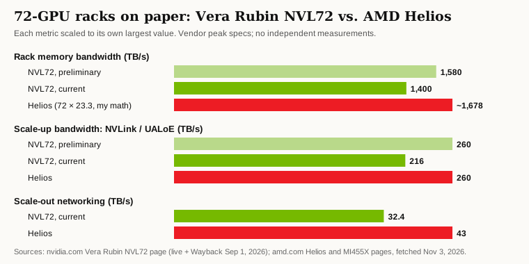
AMD's spec pages hand it a talking point. The MI455X lists 432 GB of HBM4 across 12 stacks and 23.3 TB/s of peak memory bandwidth, plus 3.6 TB/s of scale-up bandwidth (AMD MI455X). Its 72-GPU Helios rack lists 260 TB/s scale-up and 43 TB/s scale-out (AMD Helios).
On paper, after the cut (my math):
- Per GPU: 23.3 vs. 19.2 TB/s, so AMD is ~21% ahead on bandwidth, with 1.5x the memory (432 vs. 288 GB).
- Per rack: 72 × 23.3 ≈ 1,678 TB/s for Helios vs. 1,400 for NVL72, ~20% ahead. Scale-up is now 260 vs. 216 TB/s. Nvidia's old 260 TB/s figure matched Helios.
- How AMD gets there: more stacks running slower. STH says AMD runs its HBM4 at only 7.6 Gb/s per pin (STH). By my math, 12 × 2,048 × 7.6 ÷ 8 ≈ 23.3 TB/s. Running below the JEDEC 8 Gb/s target is arguably the lower-risk way to build it.
Big caveats on the AMD side:
- These are AMD's paper specs too, and AMD's own pages aren't consistent. The MI455X comparison chart still pits it against "Vera Rubin 22.0 TB/s," and one section of the Helios page lists 19.6 TB/s per GPU instead of 23.3.
- Helios is a reference design, with volume deployments "expected in 2H 2026" (AMD Helios). Rubin NVL72 is already generally available at Oracle.
- Nvidia's software stack and measured benchmarks are still the bar. Bandwidth per GPU is one input, not the scoreboard.
My take
- Bull case (Nvidia): this is a spec sheet catching up to shipping silicon, not a product getting worse. Compute and capacity hit their targets. Customers buying on measured benchmarks already got 19.2. And a lower memory bar likely means more GPUs ship sooner, which in a supply-constrained market is worth more than 13% of peak bandwidth.
- Bear case: Nvidia marketed Rubin for most of this year on 22 TB/s, then edited the pages without a word, and its own architecture blog still says 22. Decode is the workload everyone is scaling, and decode is exactly where bandwidth bites. The HGX server, the one enterprises and clouds like Oracle are buying, took a 26% cut. And AMD now leads on paper on the one spec Nvidia itself calls the decode bottleneck.
- Where I land: it's a real but modest hit, mostly to Nvidia's credibility on preliminary specs rather than to Rubin's economics. The thing to watch isn't the spec sheet. It's whether measured tokens per dollar on shipping Rubin match the marketing. If they do, this is a footnote. If neoclouds start quoting lower throughput per GPU than they promised lenders, it stops being one.
What I'm watching
- Nvidia Q3 FY27 results on Nov 17 (call at 2 p.m. PT) (Nvidia IR). Whether any analyst asks about the spec change, and what Nvidia says about HBM4 supply.
- Neocloud prints: IREN on Nov 5, CoreWeave on Nov 10, and Nebius on Nov 12 (K2 Capital, Oct 31). Whether anyone quotes Rubin throughput, or revises it.
- Updated benchmarks on shipping Rubin NVL72 and HGX NVL8 vs. AMD Helios, measured, not spec-sheet.
- Rubin Ultra's memory: ZDNet reports Samsung and SK hynix are preparing 8-Hi HBM4 for Rubin Ultra in 2Q27 instead of the original 12-Hi HBM4E plan (8-Hi means 8 memory dies per stack, not 12). That's reported, not confirmed by Nvidia (TrendForce, Oct 27). If true, it's another sign memory is setting the pace.